Introduction
Verifying the quality of optical coatings can be challenging, particularly when it comes to inspecting and controlling surface imperfections (aka scratch-dig). In addition to performance considerations, it is often a contractual requirement to apply an industry standard such as MIL-PRF-13830B and ISO 10110-7. These standards provide general methodologies for assessing whether a coating is acceptable, yet they can often raise clarification questions among inspectors, particularly where advances in coating technologies and applications continue to present new challenges.
In this article we summarise the most common coating processes, and answer frequently asked questions we receive on this topic.
FAQs Answered
1. What are the most common coating techniques?
Answer:
There are various coating techniques available, each with its own advantages and disadvantages depending on the application. Below, we detail the four most common optical coating techniques.
Ion assisted electron beam evaporative deposition (IAD): In this technique, an electron gun fires electrons at a material, vaporising it in a vacuum chamber. The vapor condenses on an optic, forming uniform layers of coating. The thickness can be precisely controlled by tuning the process. This method supports a wide range of materials and is relatively cost-effective compared to other methods.
Ion beam sputtering (IBS): Here a high-energy beam of ions bombards the desired coating material, resulting in atoms of the material “sputtering” off. The atoms expelled have high kinetic energy which causes them to form dense and smooth films on the surface of the optic. As a general rule, this method will tend to result in coatings that are cosmetically superior to IAD.
Advanced plasma sputtering (APS): This coating technique is similar to IBS, with a cathode firing plasma instead of ions. The plasma fills the entire coating chamber releasing material which is then deposited on the surface of the optic.
Plasma assisted reactive magnetron sputtering (PARMS): Here plasma is generated much like in APS, however a magnetic field confines it around the target rather than filling the whole chamber. This allows it to work at a lower pressure at higher efficiency because of the confinement of the plasma.
2. How can inspectors determine whether an imperfection is in the coating layer or the underlying substrate?
Answer:
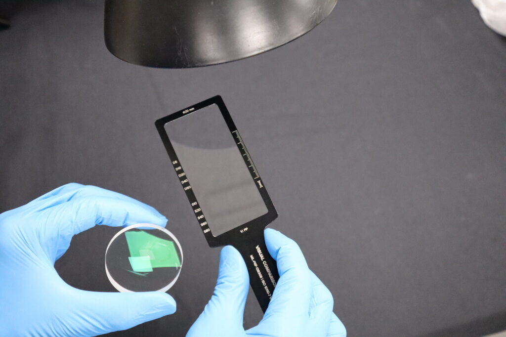
This particular question often comes up when there is a lack of reliable information on the condition of an optical surface before the coating was applied, and it is an important question to answer because understanding when and how an imperfection has been introduced can be crucial for process improvement. In short, when inspecting an optical surface for imperfections post-coating, determining which imperfections were introduced (or made worse) during the coating process can be challenging. For this reason, inspecting parts before and after coating is considered to be the most reliable and workable solution. For this application, it can be worthwhile evaluating the benefits of an automated inspection system that can automatically capture, store and display objective inspection data for quick comparison at each processing step.
3. What are the most common optical coating imperfections?
Answer:
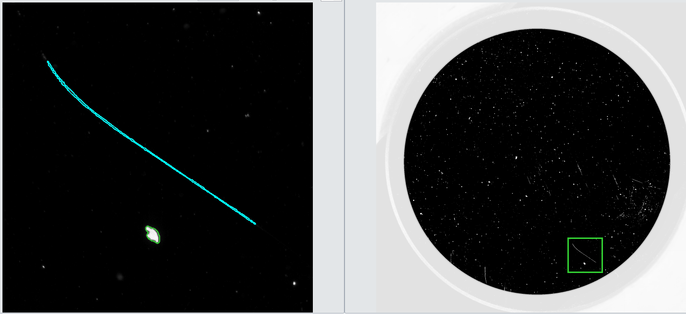
Scratches/Digs: These are linear or point-like imperfections that can scatter light and degrade optical performance.
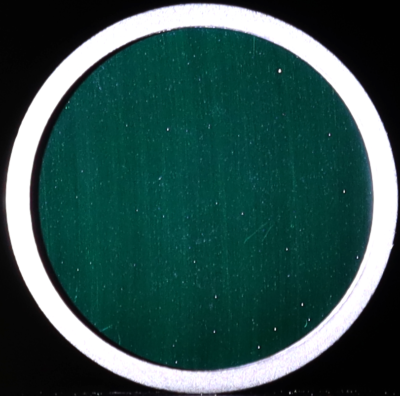
Hazing: This imperfection appears as a diffuse cloudiness, milkiness, or fogging. It is usually caused by a large number of small, point-like imperfections uniformly distributed across the surface.
Staining: Stains are discolorations or spots on the surface, typically affecting larger areas and compromising the appearance and functionality of the coating.
Pinholes: Tiny voids, holes, or missing layers in a coating which can allow unwanted behaviour such as light transmission.
4. We have certain coatings that have a milky or cloudy appearance resulting from many small and faint ‘dig’ like defects. If any of the individual digs become too large or too visible then this can be a problem. Also, it can be an issue if the level of cloudiness increases beyond a certain level. We also need to perform surface quality inspection (aka scratch dig) to a certain industry standard. How do we build a sensible, consistent and reliable inspection process around this situation?
Answer:
Many coating processes can produce intrinsic ‘dig’ like imperfections that will be deemed acceptable up to a certain level. Surprising to some, there are even applications where the presence of a uniform distribution of these small imperfections can be beneficial to laser damage thresholds, as was shown in this paper (McGuigan, Ryan & Kessler, Helmut. (2021). Thermal laser induced damage in optical coatings due to an incident pulse train. 37. 10.1117/12.2600793).
At the time of writing this article the applicable surface quality standards do not address this particular scenario. For those who require a solution today, we recommend evaluating the benefits of an automated inspection system, that is capable of handling intrinsic coating imperfections objectively and consistently.
Have another question?
If you would like to ask or submit a question which has not been covered in this article, please get in touch here:
Find out how OptiLux SD supports optical coating inspection